8085 Pin Configuration
Introduction:
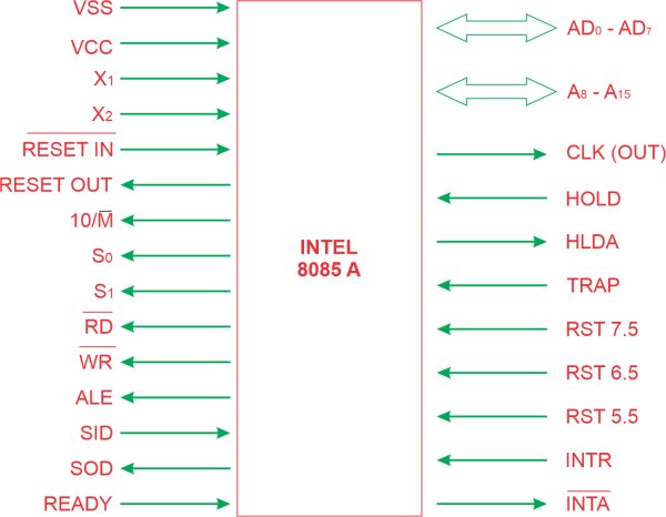
Intel 8085 is consist 40 pin IC. The pin name of 8085 is A8 – A15; AD0 – AD7; ALE; IO/M; S0, S1; RD; WR; READY; HOLD; HLDA; INTR; INTA; RST 5.5, 6.5, 7.5 and TRAP; RESET IN; RESET OUT; X1, X2; CLK; SID; SOD. The below diagram suggests the Pin diagram of Intel 8085. Now we are discussing those numerous pins.
Diagram of intel 8085 pin configuration
a) A8 – A15 (output):
These are the address buses. that are used for the maximum substantial bits or MSB of the reminiscence address like 8 bits of the I/O cope with.
b) AD0 – AD7 (input / output):
These are time multiplexed of the deal with or statistics buses, i.e. they serve a twin motive operation in 8085. AD0 - AD7 are used for the least significant bits.
The eight bits of the reminiscence deal with or I/O cope with throughout the primary clock cycle of a gadget cycle. again this records or cope with bus is used for information for the duration of the second one and 1/3 clock cycle.
c) ALE (output):
It's miles an deal with latch permit signal. It goes excessive during the primary clock cycle of a gadget cycle and allows the decrease eight bits of the address to be latched into the memory or external latch.
d) IO/M (output):
It's far a status sign which distinguishes whether or not the address is for reminiscence or I/O. while it goes high, the address on the deal with bus is for an I/O tool. when it is going low, the deal with at the cope with bus is for a reminiscence location.
e) S0, S1 (output):
These are popularity indicators sent via the microprocessor to distinguish the numerous kinds of operation, which can be given inside the underneath table
| S0 | S1 | Operation |
| 0 | 0 | HALT |
| 0 | 0 | WRITE |
| 1 | 0 | READ |
| 1 | 1 | FETCH |
f) RD (output):
It's far referred to as examine operation, and a microprocessor reads information or codes from a reminiscence area or an input tool. The microprocessor sends a sign to the reminiscence/ enter tool to manipulate the read operation.
while it is going low, the selected reminiscence or enter device is read.
g) WR (output):
When a microprocessor sends statistics to a memory region or an output tool, it's miles called a WRITE operation. Does the microprocessor ship a sign to the memory or output device to manipulate WRITE operation? while it goes low, the information at the facts bus is written into the chosen memory or despatched to the output tool.
h) READY (input):
It is a signal despatched with the aid of an input or output device to the microprocessor. This signal indicates that the enter or output device is ready to ship or receive records. The microprocessor examines the geared up sign earlier than it plays the facts transfer operation.
A gradual enter or output tool is attached to the microprocessor thru the equipped line; whilst ready is excessive, it shows that the input or output tool is prepared to send or receive statistics. whilst prepared is low, the microprocessor waits till geared up turns into high. The microprocessor examines the status of the ready signal within the second clock cycle of the machine cycle.
i) HOLD (input):
Whilst some other computer machine device calls for deal with and information buses for statistics switch, it sends a keep sign to the microprocessor. After receiving the maintain request, the microprocessor sends an HLDA (hold Acknowledgement) signal to the tool. Then the microprocessor leaves manipulate over the buses as soon because the current machine cycle is completed. internal processing may additionally maintain. The microprocessor regains manage over the buses after the preserve sign is eliminated.
j) HLDA (output):
It's far a keep well known sign despatched out by using the microprocessor after receiving the maintain signal. It's miles sent to the device which has issued the preserve sign. After removing the preserve sign, the HLDA goes low, and the microprocessor takes over the buses.
k) INTR (output):
It affords an interrupt sign. This signal offers by means of an outside device of the microprocessor. by using this line, an outside tool informs the microprocessor that it is prepared to transfer records or initiate a particular operation. The 8085 microprocessor has five interrupt strains. The INTR is certainly one of them. while it is going excessive, the microprocessor suspends the execution of its regular collection of commands. After completing the modern-day coaching, it attends to the interrupting tool. The microprocessor troubles an interrupt acknowledge signal INTA. Then it transfers information or takes any other action as required. Then it transfer data or takes any other action as required.
l) INTA (output):
The pin INTA is an interrupt acknowledge signal. The sign issued through the microprocessor 8085 after receiving an interrupt request from an external tool. The INTA is offer a lively low signal.
m) RST 5.5, 6.5, 7.5 and TRAP (inputs):
The microprocessor 8085 has 5 interrupts. RST 5.5, RST 6.5, RST 7. Five and trap are the interrupts. when the interrupt is recognized next guidance is carried out from a fixed vicinity in the reminiscence as given below:
| Line | Location from which next instruction is picked up |
| TRAP | 0024 |
| RST 5.5 | 002C |
| RST 6.5 | 0034 |
| RST 7.5 | 003C |
RST 5.5, RST 6.5, RST 7.5 are the rest TRAP is the very best priority interrupts. It's miles unaffected by way of any mask or interrupts enabled. The order of importance of the interrupts is– entice is the very best priority interrupt; INTR is the lowest priority interrupt. The interrupt precedence is like this:
- TRAP (highest priority)
- RST 7.5
- RST 6.5
- RST 5.5
- INTR (lowest priority)
n) RESET IN (input):
RESET IN is used to reset this system counter to zero. while the sign of the RESET IN pin is about too low, then this system counter is about to 0. it's also used to reset the interrupts allow and HLDA turn-flop. The RESET IN pin does now not have an effect on another flag sign in or sign in except the preparation check in. The CPU is held in reset condition as long as RESET is carried out. So, the primary characteristic of RESET is to reset the program counter.
o) RESET OUT (output):
The RESET OUT sign is used to RESET any tool or application. it's also used to reset the CPU.
p) X1, X2 (input):
X1 and X2 are terminals to be linked to an outside crystal oscillator. The crystal is connected with these two pins, which drives an inner circuitry of the microprocessor to supply an appropriate clock for the operation of microprocessor 8085. The frequency is likewise divided into elements. To function a gadget of 3 MHz, the crystal must be 6 MHz.
q) CLK (output):
The CLK signal is used to clock the gadget. It gives a clock output for the consumer. CLK can be used for other virtual included integrated circuits (IC). Its frequency is the same at which the processor operates.
r) SID (input):
SID is a records line for the serial input. The information on this line is loaded into the 7-bit of the accumulator while the RIM preparation is done.
s) SOD (output):
SID is a facts line for the serial output. The seventh bit of the accumulator is output at the SOD line when SIM preparation is completed.
Conclusion:
So, inside the above, we are brief talk the Pin Configuration of 8085. The 8085 is a forty-pin included circuit. Right here we discuss all of the pins like A8 – A15; AD0 – AD7; ALE; IO/M; S0, S1; RD; WR; READY; HOLD; HLDA; INTR; INTA RST 5.5, 6.5, 7.5 and TRAP; RESET IN; RESET OUT; X1, X2; CLK; SID; SOD. We are also put the diagram of Intel 8085 pin configuration.
We are know about the 5 interrupts which are TRAP, INTR, RST 5.5, RST 6.5, RST 7.5. TRAP is a highest priority interrupt and INTR is the lowest priority interrupt.
The input pins are AD0 – AD7; READY; HOLD; INTR; RST 5.5, 6.5, 7.5 and TRAP; RESET IN; X1, X2; SID. The output pins are A8 – A15; AD0 – AD7; ALE; IO/M; S0, S1; RD; WR; HLDA; INTA RESET OUT; CLK; SOD.
So, we recognize the pin configuration of microprocessor 8085 in short.