
8086 Microprocessor Pin Configurations
8086 microprocessor is invented and developed by Intel in 1976. The 8086 Microprocessor is an enhanced version of the 8085 Microprocessor. There are 20 address lines and 16 data lines in this 16-bit microprocessor. It is capable of storing up to 1MB. A powerful instruction set allows it to perform operations like multiplication and division effortlessly. It supports two modes of operation, namely the maximum and minimum modes. Systems with multiple processors should be set to Maximum mode, whereas systems with a single processor should be set to Minimum mode.
8086 is a 16-bit HMOS microprocessor. This microprocessor is a 40-pin dual inline package chip. 8086 requires a 5v DC power supply to perform operations. 8086 has 20 address buses and 16 line data buses. Moreover, it has multiplex lines. Out of the 20 address lines, 16 lines are used as multiplex lines. The remaining 4 lines are multiplexed with the status lines.
Pin diagram of 8086 microprocessor
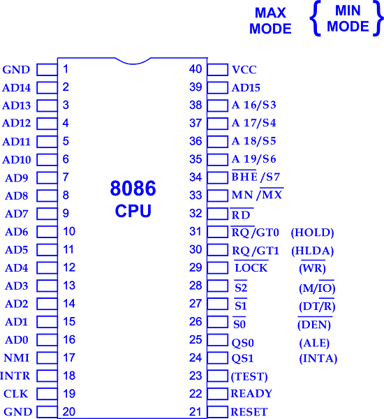
The above figure is the pin diagram of the 8086 microprocessor. As you can see from the above image, we have shown the different configurations for the minimum and maximum modes, starting with pin number 24 and continuing up to pin number 32. Nonetheless, excluding these eight pins, the rest of the 32 pins are the same for both the minimum and maximum modes, excluding these eight pins.
In the above pin diagram, we can see AD pins, which are address bus lines. Below is the explanation of these pins:
- AD0-AD15: These are address bus lines. These address lines are low-order lines. Whenever memory addresses are transmitted using AD lines, the symbol A I is used instead of AD, for example, A0-A15. When data are transmitted using AD lines, the symbol D is used instead of AD, for example, D0-D7, D8-D15, and D0-D15.
- A16-A19: These are higher-order address lines. These lines are multiplexed with the status lines. The status lines are S2, S1, and S0. Same as previous multiplexed lines. In this, if addresses are transmitted, then A16-A19 are used. Else S symbol is used for the status.
- S2, S1, S0: these are status lines that are multiplexed with the higher lines of the address bus lines. These are two pins that are active during T4, T1, and T2 states and that become passive for T3 and Tw (when ready, inactive). If the S2, S1, and S0 change during T4, S1, and S0 return to the active state. The 8288 bus controller uses these to generate the memory and input and output access control signals.
| S2 | S1 | S0 | CHARACTERISTICS |
| 0 | 0 | 0 | Interrupts acknowledge |
| 0 | 0 | 1 | Read I/O port |
| 0 | 1 | 0 | Write I/O port |
| 0 | 1 | 1 | Halt |
| 1 | 0 | 0 | Code access |
| 1 | 0 | 1 | Read memory |
| 1 | 1 | 0 | Wirte memeoy |
| 1 | 1 | 1 | Passive state |
- A16/S3, A17/S4, A18/S5, A19/S6: in addition to the specified address lines, the corresponding status signals are multiplexed.
| A17/S4 | A16/S3 | FUNCTION |
| 0 | 0 | Extra segment access |
| 0 | 1 | Static segment access |
| 1 | 0 | Code segment access |
| 1 | 1 | Data segment access |
- BHE’/S7: The bus high enable. An 8-bit device uses the BHE (Active low ) signal. The status signal is low during T1 and is used to enable data onto the most significant half of the bus, D8-D15. It is multiplexed with the status S7 signal during T1. During T2, T3 and T4 are available when the S7 pin is set. During T2, T3, and T4, the S7 signal is available.
- RD': This pin is used for the read operations. When this pin is set to 0, it performs a read operation.
- READY: The memory or slow device acknowledges that the data transfer has been completed once they have acknowledged that the transfer has been completed. The signal made available to the microprocessor by the device is synchronized by the clock generator 8284A so that the microprocessor can receive it as soon as it is ready. As you can see, the signal is active high(1).
- INTR: This pin is an Interrupt request. This is used as a triggered input. The last clock cycle of each instruction is sampled in order to determine whether the request is available during the last clock cycle of the instructions is important to note that If any interrupt requests are found to be pending, the processor will enter into the interrupt acknowledge cycle. There is an active signal high(1 ), which has been synchronized internally with the rest of the signal. After determining the interrupt enable flag, this can be internally masked after resulting in the interrupt enable flag.
- NMI: NMI stands for non-maskable interrupt. This is a type II interrupt. An edge-triggered input triggers this. The interrupt vector lookup table is located in the system memory and allows for vectoring a subroutine through a lookup table created with the interrupt vector. There is no way for software to mask NMI internally as it is not maskable. It is initiated by the transition from a low (0 ) to a high (1) point in an instruction which occurs after the current instruction. The input has been synchronized internally to ensure a smooth operation.
- INTA: INTA stands for interrupts acknowledge. It is active low(0) during the second, third, and fourth cycle of each interrupt acknowledgment of each interrupt.
- MN/MX': This is the minimum and maximum pin. This pin will indicate in which mode the microprocessor will operate.
- Rq’/GT1', RQ’/GT0': This pin is used for Request/ grant purposes. There are pins in the microprocessor that local bus masters use to force the microprocessor to release the local bus at the end of the current bus cycle that the microprocessor is running. It is important to note that each of the pins is bi-directional. In terms of priority, RQ'/GT0' has a higher priority than RQ'/GT1'.
- Lock': Local bus masters use these pins to force the microprocessor to release the local bus at the end of the microprocessor's current bus cycle at the end of their microprocessor's current bus cycle. There are a total of six pins on the card, and each pin is bi-directional.
- TEST': In this case, the 'WAIT' instruction is used to examine the situation. The processor is kept idle in the absence of a low TEST pin. Otherwise, the TEST pin will be low, indicating that the execution will continue. There is an internal synchronization of the input during each of the clock cycles on the leading edge of the clock as the clock is operating.
- CLK: CLK stands for clock input. There are two inputs for the clock input, one for the processing operation and one for the bus control activity, both of which require timing. There is a 33% duty cycle on this asymmetric square wave with an asymmetric waveform.
- RESET: This pin is used to signal the microprocessor to terminate any current activity it is performing immediately. There must be a minimum of four clock cycles between the signal being active high(1) and low(0).
- VCC: Vcc pin is used to provide the power supply, which is +5V.
- GND: GND stands for the ground pin.
- QS1, QS0: QS stands for queue status. Following is a table showing how these signals represent the status of the internal 8086 instruction queue.
| QS1 | QS0 | STATUS |
| 0 | 0 | No operation |
| 0 | 1 | The first byte of op code from the queue |
| 1 | 0 | Empty the queue |
| 1 | 1 | Subsequent byte from the queue. |
DT/R: DT/R stands for stat transmit/ Receive. This pin is required in systems that use an 8286 or 8287 data bus transceiver. Data flows through the transceiver in a particular direction.
- DEN: DEN stands for data enable.There are two pins on this pin that can be used to enable the outputs of the 8286/8287 in a minimal system that uses the transceiver. In addition to the INTA cycle, the DEN is low(0) during every access to memory and every input-output cycle.
- HOLD/HOLDA: A HOLD is an indication that another master has requested a local bus from it. This is a high(1) that is active. It is important to note that when a microprocessor receives the HOLD request, it will issue HLDA (high) as an acknowledgment in the middle of a T4 or T1 clock cycle.
- ALE: ALE stands for address latch enable. There is an address latch provided by the microprocessor to latch the address into either 8282 or 8283 address latches when a command is given. In any bus cycle, there will be an active high(1) pulse that occurs during the start of T1. Signals that are associated with ALE can never be floating, and they are always integer signals.