CarryLook Ahead Adder
What is Adder?
Adder is the combinational circuit that is used to add the bits in digital electronics. As we know, in the digital system, every number is represented in the form of binary that is 1s and 0s. In digital systems, arithmetic operations are key operations because everything in digital systems is based on the arithmetic operation.
Arithmetic operations (addition, subtraction, multiplication, and division) can be generated by only adder circuits, so the adder is the important key circuit.
If we want to add only two single bits then the circuit is called half adder.
Sum of half adder A ⊕ B
Sum of half adder A ⋅ B
If we want three bits addition then we use the full adder circuit.
Sum of full adder A ⊕ B ⊕ C
Carry of full adder A ⋅ B + C(A ⊕ B)
With the help of a full adder, we can add two numbers with multiple bits starting from the least significant bit and transferring the carry as input to the next bit's addition.
This is also called ripple carry adder, where for ith bit addition, they need the carry from (i-1)th bit.
In ripple carry adder, there is a wait for previous state sum and carry, so there is propagation delay and this makes the circuit very slow and ineffective.
So we can replace the ripple carry adder with a carry lookahead adder, where any state does not wait for the previous sum to be executed.
With the help of the carry lookahead adder, we can reduce the propagation delay and make our circuit more effective and faster.
In this adder, we use the concept of carry propagated and carry generated in each state.
Let suppose in input we have two bits Ai and Bi.
Carry generated will be Cgi = Ai·Bi
Carry propagated will be Cpi=Ai ⊕ Bi
For the ith state sum will be Si =Cpi.Ci
For the (i+1)th state carry will be : C(i+1)=Cgi+(Cpi·Ci)
Note:
So carry propagation and carry generation will only depend on the current state.
Let’s understand this with an example:
Suppose we want to add two numbers (A and B) with 4 bits each
For number A: A3 A2 A1 A0
For number B: B3 B2 B1 B0
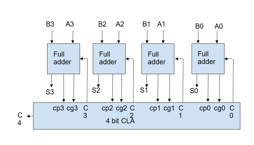
C0 will be input to the first state or first block.
For state 1:
C1 = Cg0 + (Cp0 · C0)
For state 2:
	C2 = Cg1 + (Cp1 · C1)
	C2 = Cg1 + (Cp1· (Cg0 + (Cp0 · C0)))
	C2 = Cg1 + Cp1 · Cg0 +Cp1 · Cp0 ·C0
For state 3:
	C3 = Cg2 + (Cp2 · C2)
	C3 = Cg2+(Cp2 · (Cg1 + Cp1 · Cg0 + Cp1 · Cp0 · C0))
	C3 = Cg2 + Cp2 · Cg1 + Cp2 · Cp1 ·Cg0 + Cp2 · Cp1 · Cp0 · C0
For state 4:
	C4 = Cg3 + (Cp3 · C3)
	C4 = Cg3 + (Cp3 · (Cg2 + Cp2 · Cg1 + Cp2 · Cp1 · Cg0 + Cp2 · Cp1 · Cp0 · C0))
	C4 = Cg3 + Cp3 · Cg2 + Cp3 · Cp2 · Cg1 + Cp3 · Cp2 · Cp1 · Cg0 + Cp3 · Cp2 · Cp1 · Cp0 · C0
From the above equations, we can clearly observe that for any state to generate carry, we need not to wait for the previous state carry as it is independent of C(i-1). The truth table for the carry lookahead adder is as follows:
| Ai | Bi | Ci | Ci+1 |
| 0 | 0 | 0 | 0 |
| 0 | 0 | 1 | 0 |
| 0 | 1 | 0 | 0 |
| 0 | 1 | 1 | 1 |
| 1 | 0 | 0 | 0 |
| 1 | 0 | 1 | 1 |
| 1 | 1 | 0 | 1 |
| 1 | 1 | 1 | 1 |
CLA adders must be cascaded to achieve the addition of higher-order bits. The needed number of 4-bit carry lookahead adders can be added using the carry bit to create 8-bit, 16-bit, or 32-bit parallel adders.
For instance, two 4-bit adders with additional gate delays can be used to build an 8-bit carry lookahead adder circuit layout. A 32-bit CLA is created in a similar way by cascading two 16-bit adders to create a single system.
The carry-lookahead adder's design gets increasingly complicated as the number of variables rises.
Therefore, the area is needed to grow as the variables increase and CLA is merged with IC.
When compared to a ripple carry adder, the cost of the circuitry increases as the hardware does as well.
Carry lookahead adders are used as integrated circuits that operate at high speeds, making it easier to combine adders into several circuits. Additionally, when implemented for greater bits, the increase in the number of gates is even moderate.
Although the device is faster when utilized for high-bit calculations, the circuit complexity also rises when CLAs are used. These are typically used with 4-bit modules so that they can be combined for high-bit computations.
Carry-lookahead adders are frequently employed in boolean calculations.
The carry lookahead generator's integrated circuit (IC) 74182 accepts Po, P1, P2, and P3 as carry propagate bits in an inactive low condition, Go, G1, G2, and G3 as carry generate bits, and Cn bit as an active high input. At each stage of binary adders, the active high input pin produces high carriers (Cn+x, Cn+y, and Cn+z).