Display Processor
It is a part of hardware or interpreter which is used to transform display processor code into pictures. It is used to convert digital information from CPU to analog data.
It is a digital-analog conversion which depends on the types of devices and graphics functions. The main function of display processors is called scan conversion.
In this process, contiguous graphics objects have to be separated as collections of ellipse, rectangles, and polygons.
The display processor is also sometimes called a display processing unit (DPU).
Parts of Display Processor: It has the following four parts:
- Display Controller
- Display File Memory
- Display Generator
- Display Console
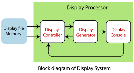
Display Controller: It is also called the Video controller. It is used to control the operations of the display device. Its functions are as follows:
- It is used to handle the interrupt.
- It is used to interpret the instructions.
- It is also used to manage time.
Display File Memory: It is used to create an image. It is also used for visual object recognition.
Display Generator: It is used to produce the character. It is also used to create curves.
Display Console: It consists of a CRT, Light pen, keyboard, and Deflection system.
Features of Display Processor:
- It is used to perform operations such as different line styles, displaying color area, and manipulating and transforming objects on display.
- Display Processors were used before the GPU (Graphics Display Processor).
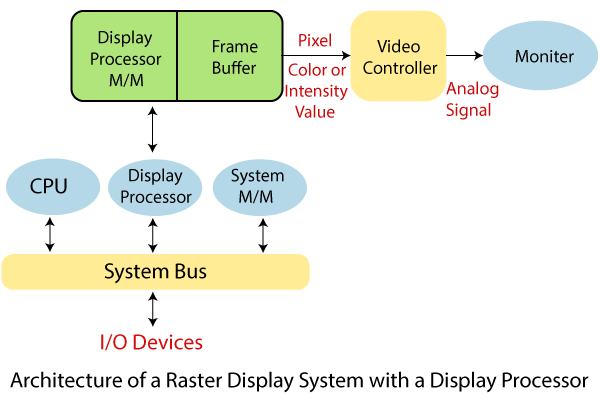
- Video Controller is the widely used Display device that is base on CRT (Cathode Ray Tube).
- The Display Processor has a separate memory area in addition to the system memory.
Working:
The video controller in the output circuit develops horizontal and vertical drive signals so that the monitosr can be scanned.
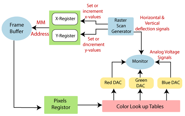
To store the coordinate pixels of the screen, we can use two registers (register X, register Y), as shown in the figure. Suppose that the value of y adjacent scan line has increased from 1 at the bottom of the screen to upward to Ymax, and the screen position or x value has increased 0 to 1 with each scan line —The position of Xmax on the rightmost side.
In a standard cartesian coordinate system, the origin is at the lowest-left corner of the screen.
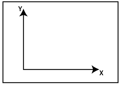
Fig: The origin of the coordinate system for the screen position recognition is usually specified in the lower-left case.
At the beginning of the fresh cycle:
The register X is set to 0, and register Y is set to Ymax. This address (X,Y`) is converted into the frame buffer’s memory address where the color value is stored for this pixel location.
The controller has received the color value (In binary form) from the frame buffer. The controller divides it up into three parts and sends every element to an individual DAC(Digital to analog converter).
In turn, these voltages control the intensity of a 3-e beam, which is focused on the (X, Y) screen position by vertical and horizontal drive signals.
For every pixel along with the top scan line, this process is repeated, each time Y increases the X register.
When the pixels are created on the first scan row through Xmax, it increases the X register. Then the X register is set to 0, and the Y register decreases by 1 to access the next scan line.
The pixels are then processed along each scan line, and the process is repeated on the last scan line (Y=0) for each scanning unit pixels are generated.
It is not directly used to control the sharpness of the CRT beam for a display system using a color lookup table buffer value.
Taking the three pixel-color value from the lookup table is used as an index. On each display cycle, this lookup operation is done for each pixel on every display cycle.
The time in the window for viewing or refreshing a single pixel is short. It takes longer to reach the frame buffer each time to read the intensity value of each pixel which is allowed:
In single access, several adjacent pixel values are put in the frame buffer and stored in the register.
A one-pixel value is shifted from the register after each acceptable time interval to control the pixel’s hot intensity.
The process is repeated with the next pixel node, and the entire pixel group will be handled in the same way.