Full Adder in Digital Electronics
A full adder is a digital circuit that performs the arithmetic operation of addition on three binary inputs (A, B, and C_in) and produces two binary outputs (S and C_out). The C_in input represents a carry-in from the previous bit position in a multi-bit addition operation, while the S output represents the sum of the three inputs and the C_out output represents the carry-out to the next bit position. A full adder is an improvement over a half adder, which can only add two inputs without considering a carry-in. The full adder is widely used in a variety of applications, including computer arithmetic, digital signal processing, and memory systems.

Construction of Full Adder
A full adder can be constructed using basic logic gates such as XOR, AND, and OR gates.
One common method of constructing a full adder is to first create two half adders, and then combine them to form the full adder. A half adder is a digital circuit that performs binary addition of two binary inputs and generates a sum output and a carry output.
Here's the construction of a full adder using two half adders:
- First half adder: The first half adder takes inputs A and B and generates a sum output S1 and a carry output C1. This can be done using an XOR gate for the sum output and an AND gate for the carry output.
- Second half adder: The second half adder takes the sum output S1 from the first half adder and the carry-in input C_in and generates the final sum output S and the final carry-out output. This can also be done using an XOR gate for the sum output and an AND gate for the carry output.
- OR gate: The carry-out output from the first half adder (C1) and the carry-out output from the second half adder (C_out) are fed into an OR gate to generate the final carry-out (C_out).
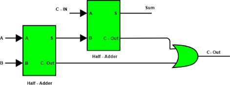
Implementation of Full adder using Half adder
A full adder can be implemented using two half adders. A half adder has two inputs, A and B, and two outputs, Sum and Carry. The Sum output is the XOR of A and B, and the Carry output is the AND of A and B.
The full adder has three inputs, A, B, and C_in (carry in), and two outputs, Sum and C_out (carry out). The Sum output is the XOR of the A, B, and C_in, and the Carry output is the OR of the AND of A and B, and the AND of the OR of A, B, and C_in.
To implement a full adder using two half adders, the first half adder computes the Sum output as the XOR of A and B, and the second half adder computes the Carry output as the OR of the Carry output of the first half adder and C_in.
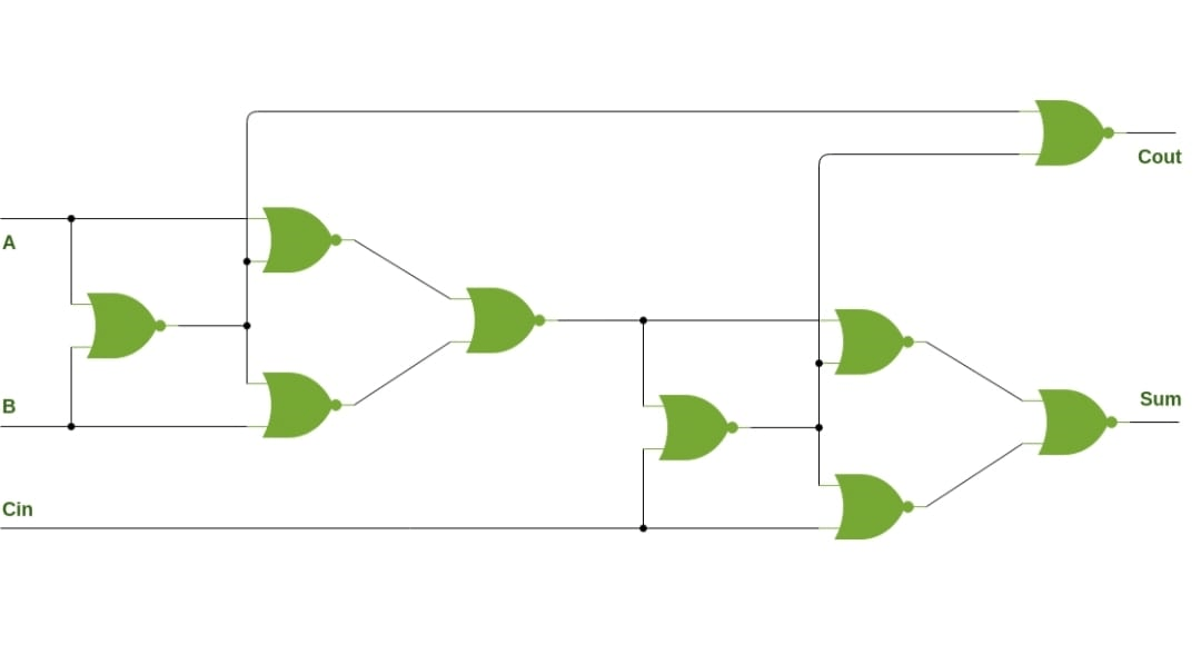
Implementation of full adder using NOR gates
A full adder can be implemented using NOR gates. A NOR gate is a type of digital logic gate that outputs a 0 if any of its inputs is 1, and outputs a 1 if all of its inputs are 0.
To implement a full adder using NOR gates, the Sum output can be obtained by connecting the outputs of three NOR gates in parallel, with one input of each gate being A, B, and C_in, respectively. The Carry output can be obtained by connecting the outputs of two NOR gates in series, with one input of the first gate being A, and the other input being B, and one input of the second gate being the output of the first gate and the input C_in.
Total nine NOR gates are required to implement a full adder
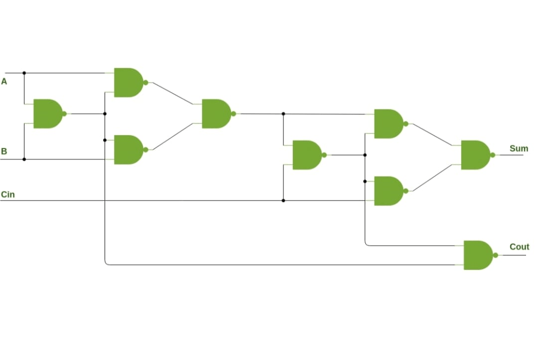
Implementation of Full adder using NAND gates
A full adder can be implemented using NAND gates. A NAND gate is a type of digital logic gate that outputs a 1 if any of its inputs is 0, and outputs a 0 if all of its inputs are 1.
To implement a full adder using NAND gates, the Sum output can be obtained by connecting the outputs of three NAND gates in series, with one input of each gate being A, B, and C_in, respectively. The Carry output can be obtained by connecting the outputs of two NAND gates in parallel, with one input of the first gate being A, and the other input being B, and one input of the second gate being the output of the first gate and the input C_in.
Working of full adder
A full adder works by combining the inputs A, B, and C_in and generating the outputs S and C_out. Here's how it works:
- Sum (S) Output: The sum S is the XOR of the inputs A, B, and C_in. XOR is a logic gate that outputs a 1 if only one of its inputs is 1 and 0 if both inputs are the same. The XOR operation allows the full adder to handle the carry-in from the previous bit addition.
- Carry-Out (C_out) Output: The carry-out (C_out) is generated as follows:
- The AND gate calculates the carry-out for A and B, which is the AND of A and B.
- The AND gate calculates the carry-out for C_in and A, which is the AND of C_in and A.
- The OR gate combines the carry-out of the two AND gates to get the final carry-out.
This allows the full adder to handle carry-over from bit to bit in a multi-bit addition operation. The carry-out can be fed back as the carry-in to the next full adder in the chain, allowing for multi-bit additions to be performed.
Full adder is designed in the following steps:
Step-01: Identify the input and output variables-
- Input variables = A, B, C_in (either 0 or 1)
- Output variables = S, C_out where S = Sum and C_out = Carry
Step-02: Draw the truth table-
| Inputs | Outputs |
| A | B | C_in | C_out (Carry) | S (Sum) |
| 0 | 0 | 0 | 0 | 0 |
| 0 | 0 | 1 | 0 | 1 |
| 0 | 1 | 0 | 0 | 1 |
| 0 | 1 | 1 | 1 | 0 |
| 1 | 0 | 0 | 0 | 1 |
| 1 | 0 | 1 | 1 | 0 |
| 1 | 1 | 0 | 1 | 0 |
| 1 | 1 | 1 | 1 | 1 |
Step-03: Draw the k-maps using the above truth table and determine the simplified Boolean expressions-
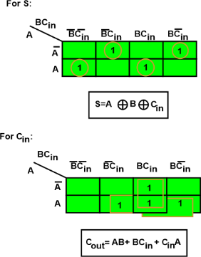
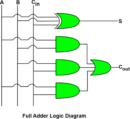
Step-04: Draw the logic diagram.
The implementation of full adder using 1 XOR gate, 3 AND gates and 1 OR gate is as shown below-
Advantages of Full Adder
The full adder is a useful digital circuit that has several advantages over other adder circuits, including:
- Ability to handle carry: The full adder can handle carry from one-bit position to the next, making it useful for arithmetic operations such as addition and subtraction.
- Improved accuracy: The full adder provides a more accurate result than a half adder, which can only add two inputs without considering a carry-in.
- Easy to implement: Full adders can be implemented using a combination of simple gates, such as AND, OR, XOR, and NOT, making it easy to design and build.
- Versatility: Full adders can be combined to form larger adders, such as a ripple-carry adder or a carry-lookahead adder, making it suitable for a variety of applications.
- Efficient utilization of resources: Full adders can be used to add multiple bits in parallel, making it more efficient than using a half adder for each bit position.
Overall, the full adder is a valuable tool in digital circuit design and has a wide range of applications in digital systems, including computer arithmetic, digital signal processing, and memory systems.
Disadvantages of Full Adder
While the full adder is a useful digital circuit, it also has some disadvantages, including:
- Complexity: The full adder is more complex than the half adder, making it more difficult to design and implement, especially for large-scale applications.
- Increased Propagation Delay: The full adder has a higher propagation delay compared to a half adder due to the additional gates and interconnections, which can impact performance in high-speed applications.
- Increased Power Consumption: The additional gates in a full adder circuit consume more power compared to a half adder, making it less energy-efficient for low-power applications.
- Increased Area Occupancy: Full adders occupy a larger area on an integrated circuit compared to half adders, making it more challenging to implement large-scale digital systems with limited real estate.
Applications of Full Adder
Full adders have a variety of applications in digital electronics due to their ability to perform binary addition with a carry-in input. Here are some specific applications of full adders in detail:
- Computer Processors: Full adders play a crucial role in the arithmetic logic unit (ALU) of computer processors. They are used to perform binary addition operations in the ALU, as well as other arithmetic operations such as subtraction, multiplication, and division.
- Memory Systems: Full adders are used in memory systems, such as dynamic random-access memory (DRAM), to perform refresh operations on memory cells and to correct errors in the stored data.
- Digital Signal Processing: Full adders are used in digital signal processing systems to perform mathematical operations on signals. For example, they can be used to perform convolution, correlation, and filtering operations on signals.
- Communication Systems: Full adders are used in communication systems, such as digital modems, to perform data transmission and error correction. They can be used to add binary numbers in order to correct errors in data transmission.
- Counter Circuits: Full adders can be used to build counter circuits, which are digital circuits that keep track of the number of events. They can be used to increment or decrement a binary number in response to a clock signal or other input.
- Cryptography: Full adders can be used in cryptography systems to perform operations on binary numbers for secure data transmission. For example, they can be used to perform modular addition, which is an important operation in many cryptographic algorithms.
- Scientific and Engineering Applications: Full adders can be used in scientific and engineering applications to perform calculations and simulations. For example, they can be used to perform numerical integration, differentiation, and matrix operations.
Note: - The full adder is generally considered more beneficial than a half adder in certain applications.
The full adder provides improved accuracy and versatility over a half adder by considering a carry-in from the previous bit position in a multi-bit addition operation. This allows the full adder to handle more complex arithmetic operations and handle carry in multi-bit additions.
However, the full adder is also more complex and slower than the half adder, making it less suitable for low-power or high-speed applications. In these cases, a half adder may be a better choice.
The choice between a full adder and a half adder depends on the specific requirements of the application, such as the size of the operands, the speed requirements, and the presence of carry-in/carry-out signals. In general, the full adder is more beneficial than the half adder when higher accuracy and versatility are required, while the half adder is more suitable when low power consumption and high speed are critical.
Conclusion
In conclusion, the full adder is a digital circuit that performs the arithmetic operation of addition on three binary inputs (A, B, and C_in) and produces two binary outputs (S and C_out). It is useful for a variety of applications, including computer arithmetic, digital signal processing, and memory systems, due to its ability to handle carry and improved accuracy compared to the half adder. The full adder can be implemented using a combination of simple gates, such as AND, OR, XOR, and NOT.
However, the full adder is more complex, has a higher propagation delay, consumes more power, and occupies more area compared to the half adder. These trade-offs must be carefully considered when selecting a full adder for a specific application. Despite its limitations, the full adder remains a valuable tool in digital circuit design and has a wide range of applications.