Working of BJT (Bipolar Junction Transistor)
Bipolar Junction Transistor (BJT)
A bipolar junction transistor (BJT) is a three-terminal device that consists of two pn-junctions constructed by placing one p-type or n-type semiconductor between 2 sets of semiconductors of different types.
BJTs' primary function is to act as amplifiers by boosting weak signals. A BJT can also be used as a solid phase switch in electrical circuits.
Types of BJT
There are two types of BJTs -
- NPN Transistor
- PNP Transistor
1. NPN Transistor
In an NPN transistor, a thin coating of p-type semiconductor is sandwiched between two n-type semiconductor materials. The base current flows from the p-type semiconductor, and the two terminals, Emitter and Collector, are removed from the two n-type semiconductors.
The arrow on the BJT symbol's emitter indicates the forward bias of the emitter and the passage of current flows through it. The usual current for NPN transistors exits the emitter as shown by the outgoing arrow.

2. PNP Transistor
A pnp transistor is made up of two p-type semiconductors and one n-type material, where a thin layer of n-type material is placed between two p-type semiconductors. The two terminals, Emitter and Collector, are taken out of the two p-type semiconductor layers, leaving just the base terminal from the n-type semiconductor. The inward arrow depicts how the normal current for pnp transistors flows into the emitter.

Working Principle of BJT
The emitter-base junction is forward-biased of BJT, while the collector-base junction is reverse-biased. Due to the emitter-base junction's forward bias, the emitter current totally flows through the collector circuit. As a result, the emitter current determines the collector current, which is nearly identical to it.
Working of NPN Transistor
It can be observed that the forward bias drives the passage of electrons from the n-type emitter into the p-type base in the forward-biased emitter-base junction and the reverse-biased collector-base junction. These electrons tend to join with the holes as they pass through the p-type base.
Only a few electrons (less than 5%) mix with the holes to form the base current because the base is narrow and lightly doped (). The remainder of the electrons (more than 95%) pass via the base region and enter the collector region to form the collector current (). In this way, the collector circuit receives the whole emitter current.
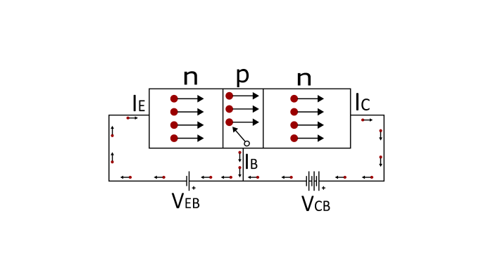
The emitter current is the sum of base and collector currents.
IE=IB+IC
Working of PNP Transistor
The emitter current in a PNP transistor is produced by the flow of holes from the p-type emitter region towards the n-type base due to the forward bias of the emitter-base junction (IE). These holes typically combine with the electrons as they cross into the n-type base region. Only a few holes (less than 5%), due to the base's mild doping and extreme thinness, interact with the electrons. Over 95% of the remainder cross the base and enter the collector zone to form the collector current (IC).
This allows the entire emitter current to enter the collector circuit. It should be underlined that current conduction is caused by the motion of holes within the pnp transistor. The power in the external connecting connections is still caused by the movement of electrons, though.
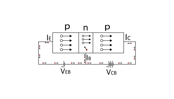
Once more, the emitter current is the result of adding the base current and collector current.
IE=IB+IC
Facts About BJT
- A BJT transistor can be thought of as a combination of two back-to-back connected diodes since there are two pn-junctions.
- Both the emitter and the base are smaller than the collector region. The base is considerably thinner than the emitter and collector. The collector of a transistor produces a lot of heat during operation, so the collector is enlarged to disperse the heat.
- Three pieces of doped semiconductors make up a transistor. The Base is the central element that forms two pn-junctions between both the emitter and collector. The inside sections are known as the Collector, while the outer ones are called the Emitter.
- The BJT's emitter-base junction is typically forward-biased, while the collector-base junction is often reverse-biased.
- When compared to a reverse-biased junction, the forward-biased junction's resistance is incredibly low.
- The emitter is heavily doped in order to provide additional electric charge (electrons or holes) to the base. The majority of the charge carriers supplied by the emitters are transferred to the collector due to the thinness and mild doping of the base. A low doping concentration can be found in the collector region.