CPU Registers
CPU Registers
Within the CPU, we have small- small storage units called registers. If we are executing a certain program within the CPU, there's a need to store that program content, we need a storage device, or small memories that reside inside the CPU called registers. Registers are small memory within the CPU used to execute instructions.
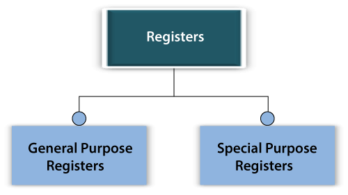
Normally, there are various types of registers used in the Central processing unit:-
- General Purpose registers
- Special purpose registers
- Accumulator(AC)
- Program Counter(PC)
- Instruction Register (IR)
- Stack Pointer(SP)
- Flag Register / Program Status Word (PSW)
- Address Register (AR) / Memory Address Register (MAR)
- Data Register (DR) / Memory Data Register (MDR) / MBR
General Purpose Registers
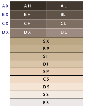
The general-purpose registers store the available content or data. At the time of different operations in the microprocessor in CPU, the general-purpose registers are used to store temporary data like input data for ALU (Arithmetic logic unit), Output for ALU, some intermediate result, any general content user wants to store in the CPU is stored in general-purpose registers. Microprocessor 8086 has eight general-purpose registers.
A detailed description of all general-purpose registers.
| Registers | Description/ Function |
| AX | AX is normally considered an accumulator of 16 bits, and it is divided into two parts of 8 bits named AH or AL. AX is used for arithmetic and logic operations. |
| BX | BX is a base register pair consisting of BH and BL. This register is used to hold the address of a procedure or to store the offset values. |
| CX | CX is a count register consisting of two parts CH or CL. It is a control register that is typically used for looping. |
| DX | DX is a data register consisting of two parts DH and DH. It is ALU for division, multiplication and input/output addresses. |
| SX | SX works like a stack pointer in the stack to point out the stack's topmost element. |
| BP | BP is a base point register among the index registers. It is a 16-bit register, and it's offset from the SS register to locate variables on the stack. |
| SI | SI is the source index register used for copying a string, and its offset is relative to the data segment. |
| DI | DI is a destination index used to find the destination for copying strings. |
| SP | SP is a stack pointer register among index registers used to locate the stack's topmost position. |
| CS | CS is a code segment register that contains the base location of the program code. |
| DS | DS is the data segment register that tells the base location for the variable of the instruction. |
| SS | SS is the stack segment register, which tells the base location of the stack. |
| ES | ES is the extra segment register that contains the additional base location for variables in memory. |
Special Purpose Registers
We store some unique content in Special Purpose registers like it holds program state(Wait, Hold, Running). Special purpose registers are also implemented in some specific microprocessors but here, we discuss the basic registers used commonly in all the systems. Let's learn registers with their working.
Accumulator (AC)
Accumulator register is used to store the result of ALU (arithmetic logic unit) operations and sometimes store one of ALU inputs.
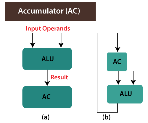
General Architecture -During operation, ALU generally required two inputs (it can be one) called operands. ALU performs operations ( like addition, subtraction, division, multiplication etc.) on the input operand, and after performing operations, ALU generates results. In basic Storage design, these results are generated firstly in Accumulator, and then further it is copied or transferred to the user requirement, it may be memory or register.
Accumulator based architecture - A specific architecture/ design of CPU says that when CPU takes two inputs, and both the inputs should be going for ALU, one of the inputs should be taken from Accumulator, and the other input can be taken from anywhere. The result of the performed operation is stored in Accumulator, and this specific design is called Accumulator based architecture.
So, we have to learn different- different kinds of architecture.
Type of Architecture (based on Input to ALU)
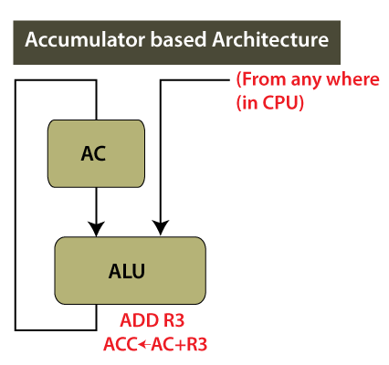
Accumulator (AC) based architecture.
Accumulator architecture says that one input should be taken from Accumulator. So here ALU takes two inputs, and one input should be necessarily coming from Accumulator and result will be copied in Accumulator and other input can be taken from anywhere (from any register R0, R1, R2, R3 ….) so CPU mention the other operands like ADD R3(from where the second operand is coming because first one is taken from the Accumulator)
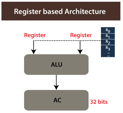
Register-based architecture
The register-based architecture says that ALU takes both the inputs from registers only. ALU takes two inputs only from general-purpose registers, and the result is generated in Accumulator. So if the CPU is using register-based architecture, then every single input is coming from registers only.
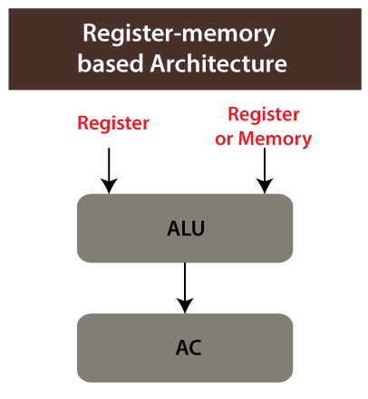
Register to memory-based architecture
In register to memory-based architecture, one of the inputs comes from the register, and the second operand can come from memory. ALU operates on both the operands.
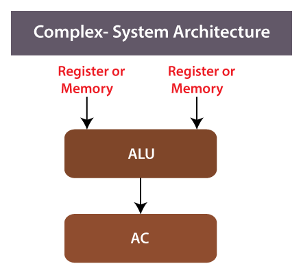
Complex System Architecture
In Complex system Architecture, inputs will be taken from anywhere. It means we can take both the input from either memory or the register. It is complex architecture as input can be taken openly, and the result is generated in Accumulator.
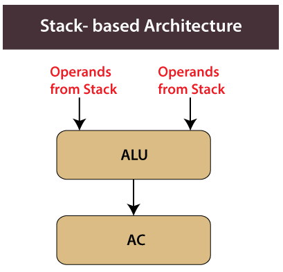
Stack base Architecture
In stack-based Architecture, both the input will be taken from the stack. Here operands are stored in stacks automatically on which operations are performed.
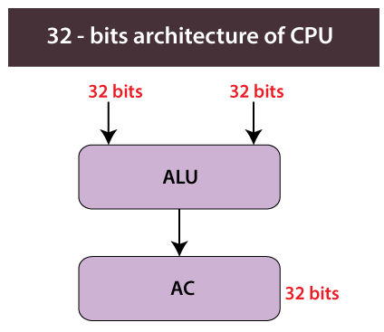
32-bit architecture of CPU
This concept says that when the CPU is implemented or designed, it has a maximum ALU capability. If ALU takes two inputs of size 32 bit each and performs operations like addition, subtraction, multiplication, and division, the system is called a 32-bit architecture system. The size of the Accumulator is based on the size of two inputs.
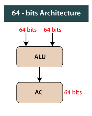
64-bit architecture
This concept also says that ALU can accept two inputs with a maximum word size of 64 and perform operations like addition, subtraction, multiplication, and division on them and generate Accumulator result. The system is called a 64-bit architecture system. The size of the Accumulator is based on the size of two inputs.
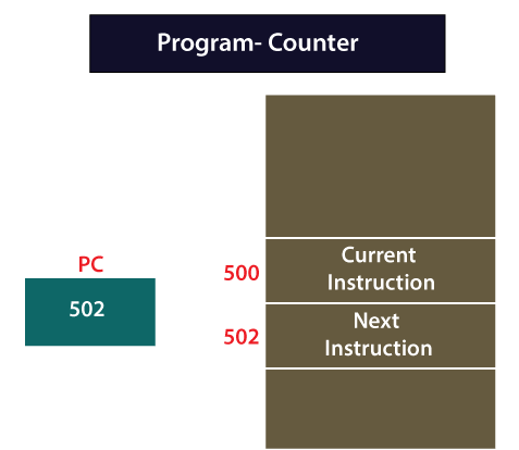
Program Counter(PC)
The program counter register is used to store the address of the next instruction. For example, the CPU is executing some instruction which is stored on address 500. Next, instruction is stored on address 502 because it can be possible that instruction takes two memory unit to execute. If the next instruction is stored at 502, then the PC's value (program counter) is 502. If this next instruction goes for execution, then the PC value changes and the next instruction is stored on a new address, and the process goes on like this.
Instruction Register (IR)
The instruction register is used to store the current instruction, executing by the CPU. The instruction register stores the current instruction fetch by CPU from memory. The IR stores this fetched instruction to execute the process.
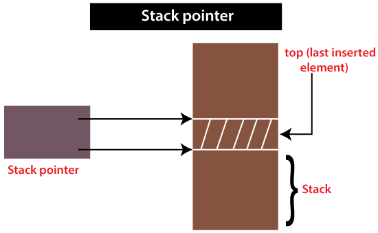
Stack Pointer (SP)
In the memory for the execution purpose, there is a stack, and the stack works on LIFO(last in first out) principle, which means that whatever element is stored last on the stack is called the top of the stack and pointed first by the stack pointer. So within the CPU, we have a stack pointer that holds the value of the top of the stack element inserted at last.
A stack pointer is used to store the address of the top element of the stack.
Flag Register / Program Status Word (PSW)
The flag register is also called a status register. As we learned before, ALU performs operations on the two input operands, and the result is stored in Accumulator, but here ALU generates two types of output. One of the outputs is generated as a result and stored in Accumulator, and the second output is the status of that result. Status is stored in the status register/flag register. The status register has a small, single bit given for one-one flag, so one flag is for S, and one is for Z.
S stands for Sign(0, 1), and Z stands for Zero( value of Z can be Set1 or Reset0)
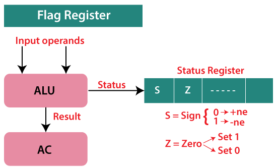
Working: Suppose, here, ALU performs an addition operation on the two input operands stored in Accumulator. The status of the result is stored in the status register. Status register/ flag register consists of many bits given to a single flag. The starting bid is given to Sign S(sign bit), which indicates the Sign flag and the second bit is given to Z(zero bit) having two conditions, Set1 or Reset 0. Now ALU thinks over the stored result whether the result is Zero or not, if addition result is zero, we set flag z as Set1 and zero flag will be reset0 when ALU result does not equal to zero.
Similarly, the sign flag indicates whether the result is positive or negative. If the sign is 0, then the result is positive, and if the sign is 1, the result is negative. So, flag/ status register is used to determine the status of the result.
Question: Why this status/ Flag register is used?
Solution: This status or flag register is used to check the conditions. For example: if we want to check if a > b or not. To check the condition, CPU will perform a function "a-b" in ALU, and the result is stored in ALU and the status of the result in the flag register; if the status of that result is positive, it means the condition is true that "a is greater than b." Such kind of conditions we write to check is based on the status/ flag register. All those condition checks written in a higher programming language are based on status register content.
Program Status Word (PSW)
In some microprocessors designs or CPU's, this PSW is only the status register. According to some other scientists in some CPU's PSW, it has been taken as a combination of two registers (Accumulator + status register). So somewhere it is known as status register, and somewhere it is known as accumulator+ status register.
Address Register (AR) / Memory Address Register (MAR)
The address register is used to send the address to memory. The address register is the originating point of the address bus. If CPU wants to send any address to memory for read or write operation then that address first comes to address register and then send through address bus to memory.
Data Register (DR) / Memory Data Register (MDR) / MBR
The data register is used to send data to Memory (Memory write) and receive data from memory (memory read). Any time data are going toward memory or coming from memory, a data register is used. In the memory, for read operation data comes from Memory to CPU, hence the data register is receiving the content through data bus and to execute memory write operation, the same data register is used to send the data back to memory through data bus.
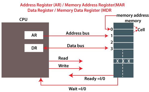
Functioning both registers:- It is a basic CPU design and can be different in some complex CPUs. There are a CPU and a memory. Nowadays, the main memory is designed to have small- small cells. The cell is the smallest part of memory, which is uniquely accessible. Each memory cell has a unique number; with that number, we can access that cell content. Cell number can start from 0, 1,2,3, 4 ……, and these cell numbers are called memory addresses. We can access these cells uniquely with these memory addresses and fetch the required data or information stored in memory very easily. Using the address bus, CPU sends requests to memory to access particular cell memory (cell 1,2,3, can be any).
Two types of operations happen in memory.
- Read
- Write
Memory read:- (i) CPU sends the address to memory using address bus.
(ii) CPU enables read control signal for memory.
(iii) Memory performs read operations and sends the data to the
CPU using a data bus.
Memory writes:- (i) CPU sends the address to memory using address bus.
(ii) CPU sends data to memory using the data bus.
(iii) CPU send enabled write signal to memory.
(iv) Write operation is performed in memory on the provided
address.
Two control bus signals, controls the operation to be performed by memory, i.e., read signal and write signal for memory. Among these signals, only one signal is enabled for the CPU to access the memory at one time. If the read signal is enabled, memory has to accept the address and read the data/content from that particular cell address, and then memory sends that content to the CPU using "data bus."
If the write signal is enabled, some data is to be written in the memory, then CPU send address and data to the memory where data is to be written using Address bus and Databus.
It is really important to find out the state of memory whether the memory is busy or free to do the CPU operations. So to tell about the memory whether it is working(busy) or free to work, "Wait signal" and "Ready signal" are used. CPU can generate these operations, initiates the memory read and memory write operations only when the ready signal(r=1) will be enabled, and the wait signal(w=0) will be disabled. Firstly, the CPU will check the ready signal is enabled; then, only the CPU will initiate these read and write operations. If the wait signal is enabled, then the CPU cannot initiate any memory operations; the CPU has to wait for the memory to get free to perform operations.