Computer: CPU (Central Processing Unit)
What is CPU? Explain its block Diagram
The Central Processing Unit is known as the central processor or main processor. The CPU is an electronic circuitry within the computer which can control the input/ output operations and carries out the instructions of the computer program by the basic arithmetic and logical unit.
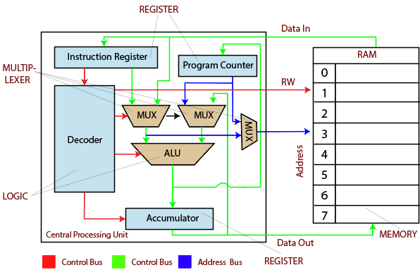
The CPU can control the instructions and data flow. The CPU contains internal memory units which are known as registers. The registers contain data, instructions, counters, and addresses. Some computers have two or more processors. The Central processing unit has two components which are given below:
The Arithmetical Logical Unit (ALU)
The arithmetical logical unit is the combinational digital electronic circuit. It can perform arithmetic and bitwise operations on integer binary numbers. The ALU is the fundamental building block of many types of computing circuits. The ALU (Arithmetic Logical Unit) has the status of inputs, outputs, or both which convey the information about the previous operation or the current operation. The ALU has three parallel data buses consist of two input operand (A and B) and the resulting output. Every data bus is the group of signals that transfer one binary integer number.
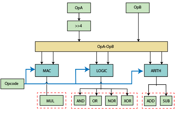
The single CPU (control processing unit), FPU (floating-point unit), and GPU (graphics processing unit) contain multiple ALU’s (logical arithmetic units). The ALU has a variety of inputs and outputs which are electrical conductors.
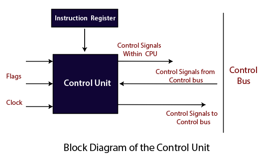
The Control Unit (CU)
The control unit is the component of the central processing unit in the computer system. It is used to control the operation of the processor. The control unit tells to computer memory that how to respond to instructions which are sent to the processor.
The Memory Management Unit (MMU)
The memory management unit is the computer hardware unit having the reference of all memories passed through it. This memory unit is used to the translation of virtual memory address to a physical address. The memory management units allowed to managing the multiple programs in single physical memory with its own address space. It is used to provide virtual addressing.
This translation process is known as memory mapping because addresses are mapped from the logical space into physical space. The memory management unit is not common in embedded systems because the virtual memory requires the secondary storage device such as a disk.
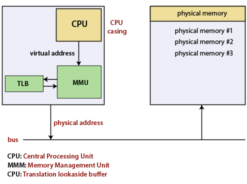
The MMU performs virtual memory management and handling memory protection at the same time. It is located within the computer’s central processing unit, and Sometimes it operates in the separate integrated chip (IC).
The memory management unit accepts the logical addresses from the central processing unit. These logical addresses refer to the program’s abstract address space but do not compare to the actual RAM location. If we add the secondary storage unit such as disk, we can eliminate the parts of the program from the main memory. In the virtual memory system, the memory management unit keeps track of which logical addresses are resident in the main memory. When the CPU requests to the address and that address is not present in the main memory, then the Memory management unit generates an exception which is known as a page fault.
Address Generation Unit (AGU)
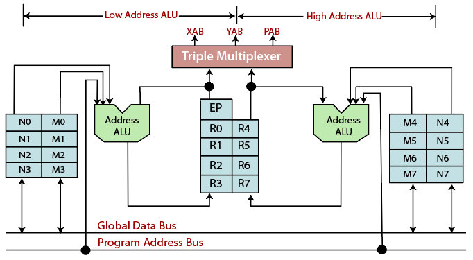
The address generation unit or address computation unit is the execution unit inside the central processing unit. This unit can calculate the address used by the CPU to access the main memory. The CPU needs to calculate memory addresses required for fetching the data from memory while performing different operations.
The Capabilities of any AGU is depended on the particular CPU and its architecture. Some CPU architecture includes multiple AGUs that’s why they can execute more than one address- calculation operation, simultaneously.
Some AGUs implement and expose the address calculation operation. The offset address and the reverse carry address operate in parallel and share common input in the AGU (address generation unit).
The only difference between the offset address and the reverse carry address is that the carry propagates in the opposite direction. Every ALU address can update one address register from its respective address register file during one instruction cycle. The value of modifier is decoded in ALU address.
The AGU operates parallel with the other chip resources, to minimize the address generation over the head. The address generation unit implements four kinds of arithmetic operations which are given below:
- Linear operation.
- modulo operation.
- Multiple wraps around modulo.
- Reverse-carry operation.
Cache
The cache is the hardware or software component in the computer memory. The cache memory can store the data so that the future request of that data can be served faster than other memories. The information which is stored in the cache memory might be the result of the earlier computation or the copy of that data, stored elsewhere.
When the system writes data in the cache, it must at some points write that data in the backing store. The cache is made up from the pool of entries. Every entry has associated information, which is the copy of the same data in some backing store.
Each entry also has the tag which specifies the identity of the data in the backing store. When the cache is checked and not found contain any entry with the desired tag, is known as the cache miss. Once the requested data is retrieved, that data is copied into the cache memory and ready for the next access.
The cache is the small-sized, volatile type of computer memory. It can store frequently used computer programs, application, and data. The cache is integrated on to the motherboard and directly embedded in the processor or main random access memory (RAM).
The Logical cache can stores data in virtual address space. The logical cache is situated in between the processor and memory management unit. The processor can access the data from the logical cache directly without going through the memory management unit. The logical cache is also called the virtual cache.
Related Posts:
- RAM (Random Access Memory) vs ROM (Read Only Memory)
- Output devices of Computer
- Input devices of Computer
- Block Diagram of Computer
- Second Generation of Computer
- Third Generation of Computer
- Fourth Generation of Computer
- Low Level Language
- Middle-level language
- Computer Software
- Computer Virus
- Memory Hierarchy
- Registers